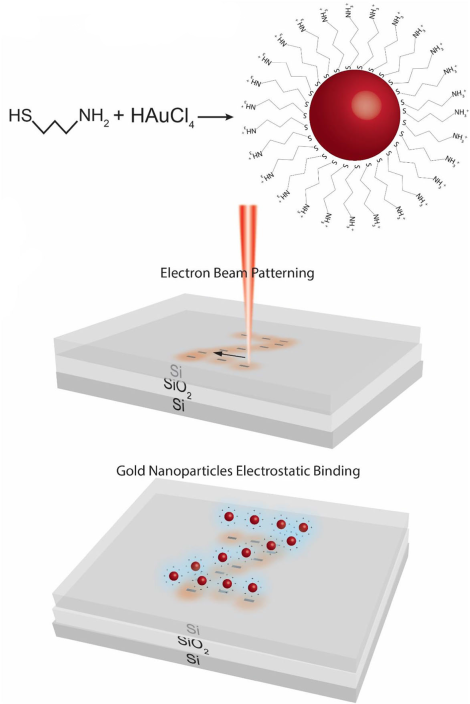
Abstract: Synthesis at the nanoscale has progressed at a very fast pace during the last decades. The main challenge today lies in precise localization to achieve efficient nanofabrication of devices. In the present work, we report on a novel method for the patterning of gold metallic nanoparticles into nanostructures on a silicon-on-insulator (SOI) wafer. The fabrication makes use of relatively accessible equipment, a scanning electron microscope (SEM), and wet chemical synthesis. The electron beam implants electrons into the insulating material, which further anchors the positively charged Au nanoparticles by electrostatic attraction. The novel fabrication method was applied to several substrates useful in microelectronics to add plasmonic particles. The resolution and surface density of the deposition were tuned, respectively, by the electron energy (acceleration voltage) and the dose of electronic irradiation. We easily achieved the smallest written feature of 68 ± 18 nm on SOI, and the technique can be extended to any positively charged nanoparticles, while the resolution is in principle limited by the particle size distribution and the scattering of the electrons in the substrate.
Keywords: Microfabrication, Patterning, Electron Beam, Colloids, Nanoparticle, Gold, Self-Assembly, Surface Potential, Nanoscale Patterns
